|

1. GaAs wafer Spec 결정 시 고려할 내용
1. Type: SC(Semi Conductor) type, SI (Semi Insulator) type이 있습니다.
2. size: 2"~4" 공급 가능
3. Orientation : <100> , <110>
4. Surface Finished : SSP (Single Side Polished)
5. GaAs devices ideal
candidates
- for high frequency and high-temperature applications in
- broadband telecommunications, data and optical
- communications, and for solar cells.
Main
Properties
| Chemical Formula
|
GaAs |
|
Molecular Weight
|
144.63
|
|
Density, g/cm3 at 300 K
|
5.32
|
|
Absorption
Coefficient, 1/cm at 10.6 μm
|
<0.02
|
|
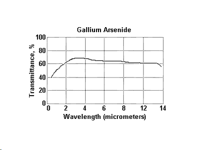
Useful
Transmission Range, μm
|
1-11
|
|
Reflection
Losses, % for 2 surfaces at 12 μm
|
45
|
|
Dielectric
Constant at 300 K, high frequency
|
10.88
|
|
Dielectric
Constant at 300 K, static
|
12.85
|
|
Melting
Point, K
|
1511
|
|
Thermal
Conductivity, W/(m K) at 300 K
|
55
|
|
Thermal
Expansion, 1/K at 300 K
|
5.7
x 10-6
|
|
Specific
Heat, cal/(g K) at 273 K
|
0.076
|
|
Debye
Temperature, K
|
360
|
|
Knoop
Hardness, kg/mm2
|
731
|
|
Young's
Modulus, GPa
|
82.68
|
|
Bulk
Modulus, GPa
|
75.5
|
|
Poisson
Ratio
|
0.31
|
|
Bandgap,
eV
|
1.4
|
|
Solubility
in water
|
None
|
Refractive
Index
|
Wavelength,
μm
|
8.0
|
10.0
|
11.0
|
13.0
|
13.7
|
14.5
|
15.0
|
17.0
|
19.0
|
21.9
|
|
Refractive
Index
|
3.34
|
3.13
|
3.04
|
2.97
|
2.89
|
2.82
|
2.73
|
2.59
|
2.41
|
2.12
| 

|
|